
Teeth Whitening: Does it work and is it safe?
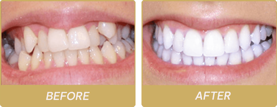
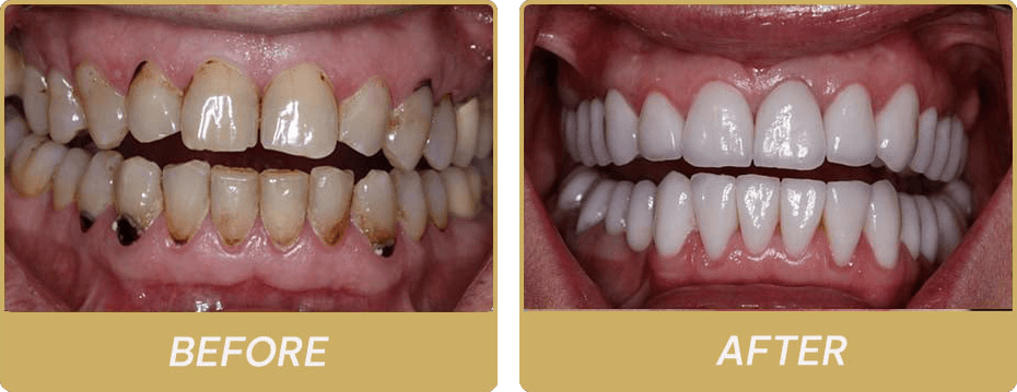
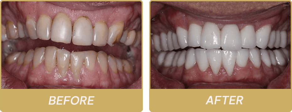
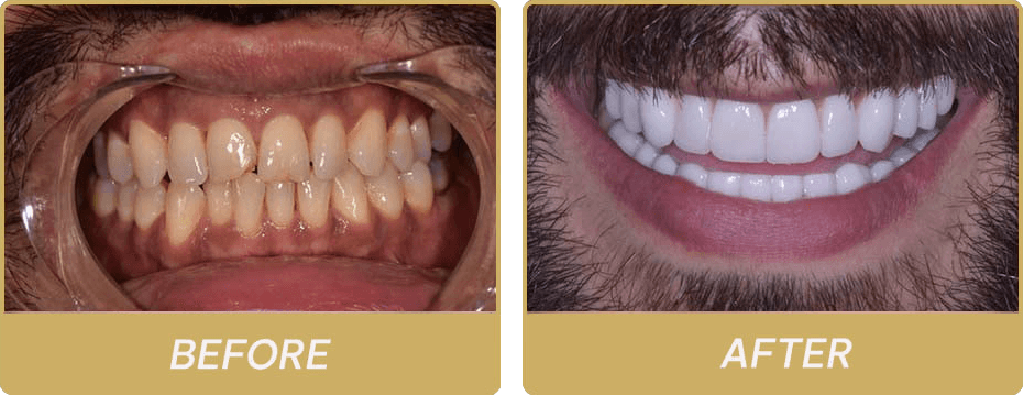
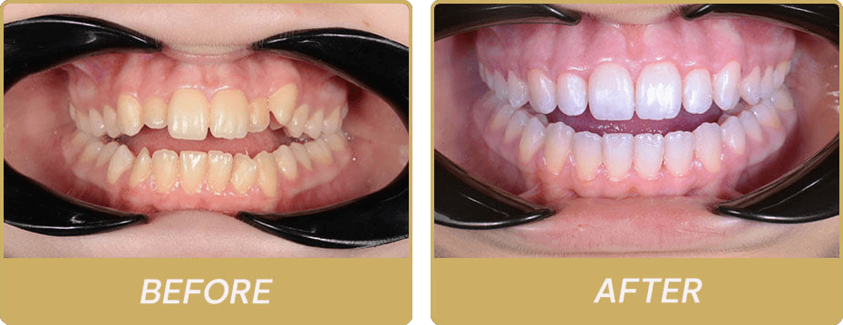
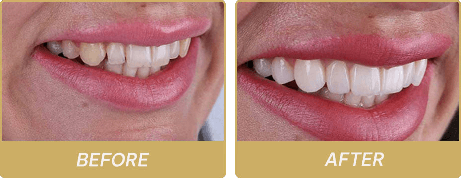
A beautiful smile and good oral health are frequently linked. Teeth Whitening in San Antonio, TX, has become a common aesthetic dentistry procedure. There

60+ Google reviews
A beautiful smile and good oral health are frequently linked. Teeth Whitening in San Antonio, TX, has become a common aesthetic dentistry procedure. There

A root canal is a dental operation that can keep a tooth from being extracted if it is severely decayed or diseased. Proper aftercare

A root canal, commonly referred to as root canal therapy, is a dental procedure that can keep a damaged or infected tooth from needing